Simulating serial communication in ngspice
Most systems today involve both analog and digital components, and digital components in a lot of cases would be communicating with each other via some form of serial communication interface (I2C, UART, SPI or any other). In such a scenario it might be useful to have a way to simulate these communications.
In this post I will be explaining an example of an ADC over SPI interface. For reference I will be taking the example of ADC081S021 which is an 8-bit analog to digital converter by Texas instruments. For simulation I will be using ngspice as a circuit simulator. Ngspice is an open source circuit simulation which allows you to build custom models of a device using the XSPICE extension. (for more details on ngspice and xspice checkout the ngspice page and user manual).
Functional details of the ADC.
In this section I will be describing the details of the ADC and its communication protocol. For reference look at the figure below, it describes the timing of adc communications. (source : https://www.ti.com/product/ADC081S021). The device works in a slave SPI mode.

Conversion
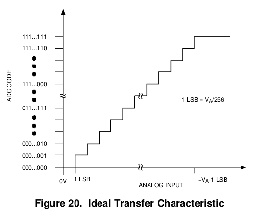
The output format for the ADC is a straight binary. LSB having a width of VA / 256. (where VA is the supply voltage to to the ADC)
Building the simulation model
I will be simulating the ADC in ngspice by building an Xspice code model of the device. The code model has two main components : the interface specification file (ifspc.ifs) and the main code model ( cfunc.mod). The ifspec.ifs file will look like this :-

each of the ports defines a pin of the ADC. SDATA , clock and CS are the pins used in SPI communication. clock is the clock pin used for synchronizing data transfer, and CS port is the chip select the pin.
the function model in the cfunc.mod file is given by-
Now that we have completed the code we can compile it along with ngspice. To do that simply go the the ngspice folder and type "make" then "sudo make install". Now we can type simulate this like a normal component of a circuit. (refer to ngspice manual for more details)
The example netlist file is :
Simulation and results :
the result of the simulation are shown in the figure below:

At t=3 the chip select line goes low. In the next rising edge (t=4) the transmission starts. The first 3 bits are leading bits which are zero. The next 8 bits are the data (the voltage converted to digital). Th voltage we have applied is 8V dc voltage. The digital converted value will be
data = Vin x 255 / Va
= 8 x 255 / 10
= 204 = (converting to hex) 0xCC
The transmission is LSB first. 0xCC in binary is (0x11001100), so the transmitted bits would be (0 0 1 1 0 0 1 1) which can be seen in the figure. The last 4 bits are trailing bits which are zero.
This is a basic example of how devices with serial communication can be simulated in ngspice (this model should be compatible with LTSpice too). I will be trying to build models or more such devices and maybe a general SPI debugger model which can be used anywhere.
Note : I have kept the clock input as 5 and other digital inputs as 10 to maintain clarity in the plots. The plot is not of very good quality as I am using the built in plotter of ngspice which is very basic. Next time on, I can try to export the data to file and plot using python. I will also be trying to complete this code model by including all the electrical characteristics f the device (max dc power, pin impedance, minimum timing requirements etc.).


Comments
Post a Comment